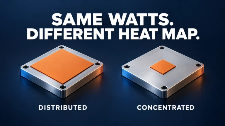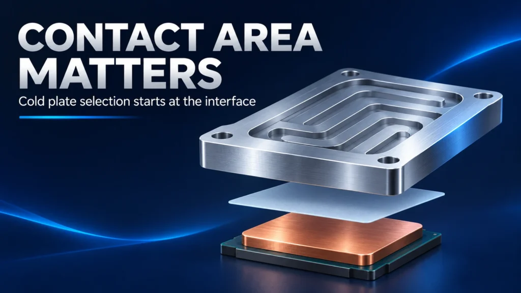
Chip contact area affects the local path from the device into a cold plate, so it belongs in initial selection alongside heat load, temperature limits and coolant conditions. A plate that covers the package outline can still have an unsuitable contact stack or inadequate performance under the actual heat-source footprint.
Start by identifying the surface that physically contacts the thermal interface material, or TIM. Then screen candidate plates for mechanical fit and relevant thermal evidence. The objective is a defensible shortlist and validation plan, not a guaranteed temperature derived from area alone.
Identify the area that actually transfers heat
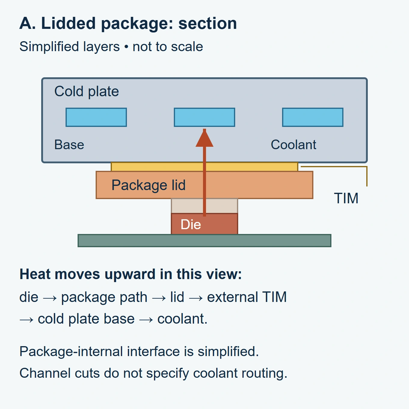
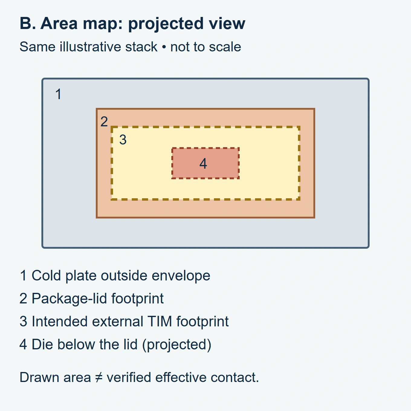
Die area, package-lid area, TIM footprint and cold plate outline are different dimensions. A lidded processor transfers heat through its package structure before it reaches the external interface. A direct-die arrangement has different contact and loading constraints. Do not substitute one area for another just because both appear in a component drawing.
- Device boundary. Identify the exact device and revision, whether it is lidded or exposed, and the approved cooling interface.
- Contact geometry. Mark the intended mating surface, its usable footprint, height and orientation on the drawing.
- Heat input. Associate the power and spatial distribution with that surface and operating case.
- Temperature criterion. State whether the limit refers to junction, case or another defined measurement node.
The visible lid may spread heat beyond the die, but that does not establish uniform heat flux across the lid. Similarly, covering the full package outline does not prove uniform contact pressure. Use the component manufacturer’s mechanical and thermal requirements to identify the relevant interface before requesting a plate comparison.
Our heat-source map article explains how to document locations and operating scenarios. Here the narrower task is deciding whether a candidate plate and mounting arrangement can use that contact footprint effectively.
Separate nominal coverage from a usable contact stack
In an ideal uniform layer, conduction resistance varies as thickness divided by conductivity and area. This explains why increasing the effective contact area or reducing an excessive bond line can matter. It does not supply the complete interface resistance: contact at both surfaces, flatness, pressure distribution, voids and material behavior also influence the installed result.
A larger outside plate dimension does not automatically enlarge the effective device interface. Heat still has to spread from the source into the plate and reach the cooled region. Increasing base thickness may help spreading in some geometries while adding conduction distance and mass. The balance requires geometry-specific analysis or evidence; neither the thinnest nor the thickest base is a universal choice.
Screen the contact stack before selecting a plate
Swipe the table horizontally to compare all columns.
| Drawing or assembly item | Initial selection question | Evidence needed |
|---|---|---|
| Contact footprint | Does the usable mating face cover the intended interface? | Controlled device and plate drawings |
| Heights and tolerances | Can all intended sources contact without excessive loading? | Stack analysis and assembly limits |
| TIM | Is its installed condition suitable for the actual gap? | Material guidance and bond-line basis |
| Mounting | Can the approved load be applied without damaging the package or board? | Load limits, supports and assembly method |
| Internal cooled region | Is it positioned to serve the source footprint? | Relevant geometry and thermal evidence |
For multiple devices, the tallest component can carry the clamp load while another receives a thicker interface or loses contact. A nominal CAD fit does not resolve that tolerance case. Review the extremes with the mechanical owner before selecting channels or asking for a stronger pump.
Compare performance data at the same source boundary
A thermal-resistance value is useful only when its temperature nodes, heat input and operating conditions are defined. A value measured with a large heater cannot automatically be assigned to a small chip footprint. Spreading and interface conditions may be different even if coolant inlet temperature and total watts match.
Eaton’s custom cold plate guidance distinguishes uniform and concentrated heat inputs and discusses surface-temperature requirements. This supports requesting the source geometry behind a performance claim rather than choosing solely by a nominal power rating.
- Match the source. Compare heater footprint, source position, load distribution and contact construction with the intended device.
- Match the conditions. Record coolant composition, inlet temperature, flow, pressure-drop measurement boundary and mounting method.
- Match the result. Identify the temperature node and uncertainty. Determine whether the result supports the required limit or leaves a device-level measurement unresolved.
If the boundaries differ, request an analysis or test that explains the difference. Do not rescale a published thermal resistance by the ratio of contact areas and treat the result as a validated product rating. The simple inverse-area relation for one uniform layer does not describe the whole plate and device stack.
Keep contact decisions connected to the liquid circuit
Concentrated heating can make channel location and local heat-transfer behavior important. Moving a channel or increasing internal surface area may also change pressure loss, base stiffness, manufacturing access or sealing features. A candidate that performs well at a prescribed laboratory flow still needs that flow in the installed circuit.
Boyd’s cold plate technical datasheet describes geometry optimization together with thermal and hydraulic validation. Its listed designs and ratings belong to Boyd; they are not ThermalBro specifications. For your comparison, request the candidate’s pressure-drop behavior and reconcile it with the pump or external supply available at the plate boundary.
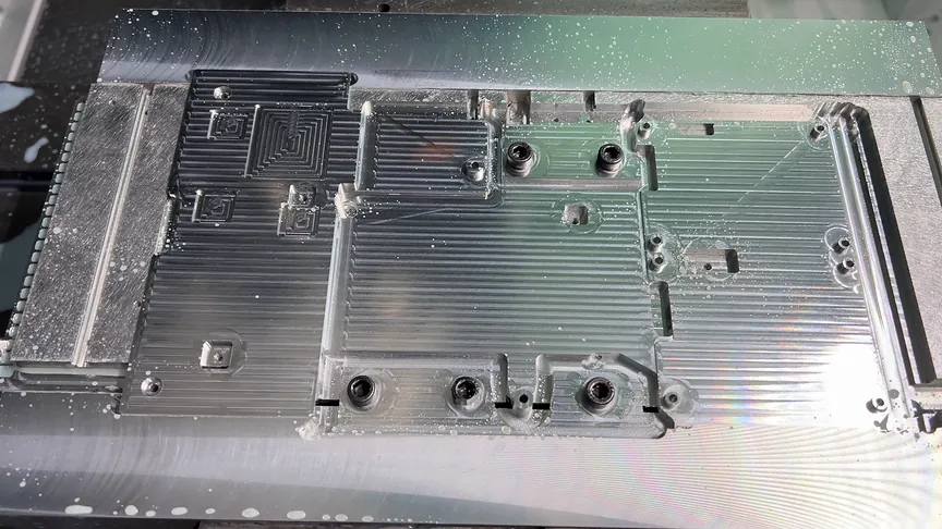
Our cold plate CNC design guide connects this review to controlled drawings and manufacturing scope. Specify whether the request covers a machined part or also includes joining, sealing, cleaning, assembly and testing.
Use a changed-footprint example to screen candidates
Keep the candidate
The mating face and mounting can meet the device requirements, and relevant evidence supports the new heat footprint under available coolant conditions. Complete the agreed installed validation.
Revise or reject it
Contact is lost at a tolerance extreme, the mounting load is unsuitable, or the required thermal result cannot be achieved at available flow. Address the limiting interface before comparing price.
An unresolved thermal result is not proof that the candidate fails. It is a reason to keep selection conditional. A new base geometry or mounting feature may require drawing changes, a prototype and additional inspection, so include that work when comparing the cost and schedule of reuse against redesign.
Define the prototype evidence before freezing the design
Validate the intended contact construction, not only the total heat balance. A fixture should represent the source footprint and location, interface material and mounting condition where they affect the conclusion. Record any difference from the final device and the limits of the fixture result.
Link prototype evidence to design changes
Swipe the table horizontally to compare all columns.
| Validation question | Record with the result | Reopen the review when |
|---|---|---|
| Does the device meet its limit? | Defined temperature node and relevant load cases | Package, load distribution or limit changes |
| Is contact repeatable? | Build revision, TIM application and mounting method | Heights, supports or assembly method change |
| Are liquid conditions achievable? | Plate inlet temperature, flow and pressure drop | Fluid, pump, hoses or branches change |
| Does the evidence cover production? | Drawing/BOM and tested construction | Material, joining route or critical geometry changes |
Repeat assembly or tolerance-focused checks when they are needed to address contact variability; the responsible validation team should choose the sample scope. A single convenient prototype does not establish every production tolerance combination. Keep local temperature evidence alongside fluid measurements, because a plausible coolant energy balance can coexist with an overheated source.
For an initial CNC machining review, send the 2D/3D revision, contact map, material, critical dimensions, mounting constraints and quantity stage. Include the fluid boundary and identify the thermal evidence you need. ThermalBro’s drawing-based supply scope must be agreed separately from the system owner’s final device acceptance.
Questions before choosing a contact footprint
Should the plate be exactly the size of the chip?
Not necessarily. Mounting, sealing, fluid passages and heat spreading may require a larger envelope. The important distinction is between the outside envelope and the usable thermal interface. Check both against the actual package and installation.
Can a thicker thermal pad make an incompatible plate fit?
Only if the selected material and assembled gap meet the thermal and mechanical requirements. Adding thickness can bridge a gap while increasing thermal resistance or changing loading. Treat the altered stack as a design change requiring evidence, not a universal fit correction.
What if the device supplier has not released the mechanical drawing?
Request controlled interface information or a clearly identified provisional envelope. Mechanical packaging work may continue under assumptions, but contact compatibility and temperature acceptance remain open until the required package data and validation are available.